Glide Write offers full support in your Lithography, Etching and DLC Coating needs.
 Photo-Lithography
Consist of 3 major steps.
- Patterning: Expertise in patterning process using spin on Photo-resists. We can achieve the Photo-resist thickness between 10um to 120 um. Determine the rate and speed of dispense to achieve the desired thickness. We have worked with many different type of Photo-resists and can recommend to suit individual application.
- Exposure: Using state of the art Karlsuss MA-6 contact aligner on mask size of 4, 5 or 6 inch diameter at 240nm & 365nm wavelengths.
- Develop: Break down resist polymers by using the appropriate developer. After these steps the parts is ready for the etching process.
 Etching
Etching can be done on various type of ceramic substrates with stable and repeatable results. Extensive experience in Dry etching by ICP (Inductive Charged Plasma) on ceramics wafers. Depending on the substrate material etch depth can be achieved up to 10um and beyond. We take ownership of projects from start to finish to meet each customer’s requirement.
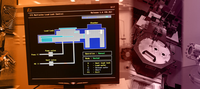
- STS Dry etch IPC (Inductive Charged Plasma).
- Gas use: CF4 (etch) and O2 (clean)
- Capable of deep etch.
 DLC (Diamond Like Coating)
We have extensive experience in this process. Protect the surface of the part or component with a diamond like coating to increase the toughness to resists wear cause by friction.
- Our DLC can be applied with or without the Si seed layer.
- The DLC layer can be accurately controlled from 50 A to 1000 Angstroms.
- Proven strong bond and resist mechanical wear.
- STS IPC (Inductive Charged Plasma)
- Capable of depositing 50A-1000A of DLC on parts/substrates.
- Gas use: CH4 (DLC) and O2 (clean)
- Coated layer to protect parts from rusts, wear and tear. Extended usage shell life.